In today’s electronics manufacturing, precision is everything. And well, sometimes even the most well-engineered circuit can underperform if something goes wrong during assembly? That’s why PCB assembly quality control is such a big deal in modern electronics manufacturing. Today’s PCBs are not bulkier like the old times. Today, you will see how they are smaller, denser, and more complex than ever. All the components are packed tightly, solder joints are microscopic, and many critical connections are completely hidden from view.
But guess what? Many companies still rely only on manual inspection or basic testing, which, truth be told, are not enough anymore. This is where technologies like automated optical inspection, PCB assembly, and X-ray testing in PCB assembly come into play.
Together, these inspection methods can detect the errors early, reduce rework, and make sure that boards leaving the factory are reliable for your end user. In this article, we will tell you all you need to know about what an aoi, how X-ray inspection works, and how both contribute to best practices for high quality pcb assembly. Let’s get started!
What Is AOI, and why does it matter?
Let’s begin with the basics of it: What is an AOI?
AOI stands for Automated Optical Inspection. In simple terms, it’s a camera-based inspection process that automatically checks assembled PCBs for visible defects. So instead of relying on human eyes, an automated optical inspection system uses high-resolution cameras and software to compare each board against predefined standards.
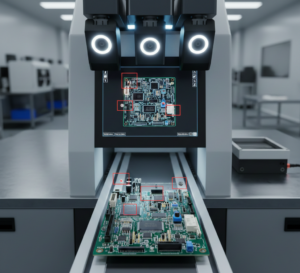
In automated optical inspection PCB assembly, the system actually scans the board after every key stage and looks for issues such as missing components, wrong placement, polarity error, or poor solder joints. Thanks to the automation, it’s actually pretty fast, repeatable, and far more consistent than human hands and eyes.
So AOI matters in PCB assembly quality control because:
- It detects defects that are hard to see with the naked eye
- It reduces dependence on manual inspection
- It improves consistency across large production volumes
- It helps manufacturers maintain stable yields
An automated optical inspection system also creates inspection data that can be analyzed over time. So that’s another benefit!
The Role of X-Ray Testing in PCB Assembly
Here comes the part where it gets a bit complicated. There is no doubt that AOI is powerful. But it has its limitations, which cannot be looked over with high-risk industries. AOI can only inspect what the camera can see. What about the modern PCB designs that often include components like BGAs (Ball Grid Arrays), QFNs, and multi-layer boards, where solder joints are completely hidden underneath components? This is where X-ray testing in pcb assembly becomes more important than ever.
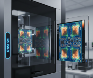
It works just like anyone would imagine an X-ray machine working. In this case, an X-ray inspection system for pcb allows manufacturers to see inside the board without damaging it. You can see internal structures, solder joints, vias, and connections that are never visible from the surface.
With X-ray testing in PCB assembly, manufacturers can even detect:
- Hidden solder voids
- Cold or insufficient solder joints
- Bridging under BGAs
- Internal cracks or misalignments
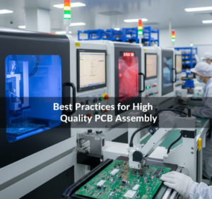
Best Practices for High Quality PCB Assembly (with AOI + X-Ray)
-
Inspect Early and Often
One of the most overlooked aspects of PCB assembly quality control is the timing. Most of your EMS partners will treat inspection as their final step, and something to check once the final product is there. But what if that’s when you find the faulty part? That means more money, more repairs! In automated optical inspection pcb assembly, AOI is often placed immediately after solder paste printing and reflow soldering. This actually allows defects to be caught when they’re still easy to fix.
E-ray inspection is also used for complex and high-risk assemblies to make sure no defect can slip through.
-
Use the Right Inspection for the Right Board
Not every PCB needs X-ray inspection, but many modern designs do. Here is a good rule of thumb you should take note of:
- Use AOI for all SMT assemblies.
- Use X-ray testing in pcb assembly for BGAs, fine-pitch components, and multilayer boards.
This is a targeted approach that will help to balance quality and overall efficiency!
-
Analyze Inspection Data, Not Just Pass/Fail
Another thing to note here is that both AOI and X-ray systems generate valuable data. Instead of using them only for rejection, manufacturers should analyze trends like recurring defects, solder inconsistencies, or placement drift. This is a feedback loop that will make your PCB assembly quality control systems stronger and help you improve!
-
Work with a Manufacturer That Takes Inspection Seriously
Last but not least, Inspection tools are only as effective as the processes behind them. Manufacturers like Karkhana.io integrate AOI and X-ray inspection into their overall EMS workflow. This way, we ensure consistent quality rather than treating inspection as an afterthought. So yes, here we value both automated optical inspection and PCB assembly, and X-ray testing in PCB assembly!
Final Thoughts
If we talk about today’s scenario around electronics, then quality is not “optional.” Its a non-negotiable and pretty much expected by the end user. And as PCB designs become more compact and complex, relying on traditional inspection methods simply isn’t enough. What you need is technologies like automated optical inspection, PCB assembly, and X-ray testing in PCB assembly. They are clearly far more functional and reliable!
Understanding what an AOI is, how an automated optical inspection system works, and when to use an X-ray inspection system for PCBs will help businesses like yours to make smarter decisions about their products. Now you know the best practices for high-quality PCB assembly, and how it’s the key to success. At Karkhana.io, that’s exactly what we take pride in, and take PCB assembly quality control as a priority!
Frequently Asked Questions
1. What is AOI in PCB assembly?
You can think of AOI as an extra set of very sharp, very patient eyes on the production line. In PCB assembly, things move fast. So, instead of a person manually checking every tiny component, cameras and software do the job automatically. In automated optical inspection pcb assembly, the system scans the board and compares it with a reference design to spot anything that looks off.
2. How does X-ray testing help in improving PCB quality?
Some of the most critical PCB defects are the ones you simply can’t see from the outside. This is where X-ray testing in pcb assembly becomes incredibly valuable. X-ray inspection allows manufacturers to look inside the PCB without damaging it, revealing what’s happening beneath the surface.
3. Why is AOI important for surface-mount technology (SMT) assemblies?
SMT assemblies pack a lot of components into very little space. An automated optical inspection system brings consistency to the process. It checks every board the same way, every time, without fatigue or oversight. So it quickly flags placement issues, solder defects, or missing components that could otherwise slip through, making it pretty important for PCB assembly quality control.
4. What types of defects can X-ray testing detect that AOI cannot?
X-ray testing in pcb assembly fills that gap by revealing defects that are hidden inside the board. With an X-ray inspection system for PCBs, manufacturers can detect solder voids beneath BGAs, internal cracks, insufficient solder joints, and alignment issues that are impossible to catch visually.
5. Do all PCB manufacturers use both AOI and X-ray inspection?
Not necessarily. Some manufacturers rely only on basic inspection methods, especially for simpler products. However, those that follow best practices for high-quality PCB assembly usually combine both AOI and X-ray inspection.