PCB assembly can account for 30–50% of your total product build cost, and in high-mix or low-volume projects, that percentage often creeps even higher. When margins are tight and time-to-market matters, understanding pcb assembly cost drivers—and how to rein them in—can make or break your product’s success.
At Karkhana.io, we help hardware teams optimize every rupee spent on PCB assembly without sacrificing quality or reliability. In this post, we’ll walk through the major cost drivers in PCB assembly and share practical strategies for controlling each one, so you can build smarter, faster, and leaner.
1. Component Costs: The Biggest Line Item
Components—ICs, passives, connectors, and electromechanical parts—typically make up 40–60% of your PCB assembly bill of materials (BOM). Popular microcontrollers, power management chips, or even specialized sensors can carry premium price tags, especially when sourced in small quantities, directly impacting the pcb assembly cost per component.
How to Control It
- BOM Rationalization: Audit your component list to remove duplicates or unnecessary features.
- Alternate-Source Planning: Identify second-source compatible parts (e.g., use two different MOSFETs with similar specs) to avoid allocation risks and benefit from competitive pricing.
- Volume Discounts & Forward Buy: Lock in larger orders at negotiated prices or use buffer stock models to hedge against price spikes.
- Standardization: Wherever possible, standardize on common resistor, capacitor, or connector families to leverage bulk pricing across multiple projects.
2. PCB Fabrication
The bare PCB cost varies with board size, layer count, material (FR-4 vs. high-TG vs. Rogers), and finishing options (ENIG, HASL, etc.). Exotic stack-ups and tight impedance requirements drive up fabrication costs dramatically.
How to Control It
- Optimize Layer Count: Consolidate signals and planes to minimize unnecessary layers.
- Panel Utilization: Design boards to fit efficiently on standard panels (e.g., 18″ × 24″) to reduce per-unit cost.
- Material Trade-Offs: Only specify high-TG or specialized substrates where absolutely required—stick with FR-4 for most applications.
- Standard Finishes: ENIG is reliable, but HASL or OSP can be more cost-effective for non-mission-critical surfaces.
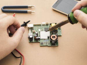
3. Assembly Process: Labor, Setup, and Machine Time
SMT pick-and-place, wave soldering, selective soldering, conformal coating, and manual work all incur machine time and labor costs. For product portfolios with frequent variants, mixed model pcb assembly services can significantly influence setup efficiency and overall cycle time.
How to Control It
- DFM for Assembly: Optimize footprint sizes, avoid 01005 passives unless necessary, and group similar components to minimize nozzle/tool changes.
- Panelization Strategy: Batch boards into panels that maximize machine throughput while maintaining standard rack sizes.
- Automated vs. Manual Balance: Leverage automation for high-volume repetitive tasks but reserve manual labor for low-volume or complex assemblies.
- Quick Changeover Techniques: Use common feeders and smart line configurations to reduce setup times between different PCBs.
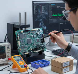
4. Testing & Quality Assurance
Every test station—ICT (In-Circuit Test), functional test, burn-in, or AOI/X-ray—has an associated capital amortization and per-unit operation cost. Excessive test steps or high reject rates can spike your per-unit expense.
How to Control It
- Risk-Based Testing: Map out failure modes and apply only the tests needed to ensure reliability, rather than blanket coverage.
- Inline Inspection: Use 3D AOI early in the line to catch defects before they cascade into costly rework later.
- Yield Improvement Programs: Analyze SPC data to identify chronic failure points and implement corrective actions, reducing rework and scrap.
- Modular Test Jigs: Invest in flexible, scalable test fixtures that can be quickly reconfigured for new designs.
5. Scrap, Rework & Yield Losses
Even a 1–2% yield loss on a 10,000-unit run can translate to hundreds of boards scrapped or reworked, at full cost for materials, assembly, and testing.
How to Control It
- Root-Cause Analysis: Treat every failure as a learning opportunity; track defects by type and implement process or design changes.
- Process Standardization: Document best practices in SOPs and train operators to reduce variability.
- Preventive Maintenance: Keep pick-and-place heads, solder nozzles, and reflow ovens in calibration to avoid drift-related defects.
- Real-Time SPC: Monitor critical parameters (e.g., solder paste volume, placement accuracy) with dashboards that trigger alerts before yields degrade.
6. Overhead & Supply Chain Logistics
Warehousing, inbound inspection, customs duties, packaging materials, and freight can cumulatively add 10–15% to your landed cost, especially if you’re shipping small batches or importing critical parts.
How to Control It
- Consolidated Shipments: Combine PCB runs and component deliveries to reduce freight overhead.
- Local Sourcing: Leverage Karkhana.io’s 600+ vetted suppliers in India and SEA to minimize import duties and transit times.
- Vendor-Managed Inventory (VMI): Align safety stock levels with consumption to balance inventory carrying cost against stockout risk.
- Lean Packaging: Use recyclable, right-sized packaging to cut material cost and reduce dimensional weight pricing.
7. Design Complexity & Customization
Exotic features—like HDI, blind/buried vias, gold-finger edge connectors, or rigid-flex—introduce premium charges in both fabrication and assembly.
How to Control It
- Feature Justification: Only deploy advanced features when the performance benefit clearly outweighs the cost penalty.
- Modular Architectures: Design a core PCB platform that can support multiple variants with minor add-on boards or plug-in modules.
- DFX Reviews: Conduct Design for Cost (DFC) as rigorously as DFM—question every special fabrication or assembly step.
Conclusion
Reducing your PCB assembly costs isn’t about cutting corners—it’s about making informed trade-offs at every stage of design, sourcing, and production. By applying DFM/DFC reviews, smart panelization, risk-based testing, and supply chain optimization, teams can achieve cost efficient pcb assembly without compromising quality.
At Karkhana.io, we partner with you to identify and tame these cost drivers—using our turnkey electronics manufacturing services, deep supplier network, and real-time process data to help you build cost-efficient, reliable products at scale.